PCB Crown::Build History
Conception
The idea came out of some discussions around the OSH Park offices, which for a couple reasons got steered toward making Laen a cool electronic hat. Since he’s a fan of neat art projects, we looked at various projects, and decided that with the lovely OSH Park purple, we could make him a crown fit for a King (of PCBs). It seemed like this would be a reasonable team effort, and totally wouldn’t be possible without help and knowledge from Cat and Kelly, fellow dwellers of the purple pcb mines.
Initial concept
Before even committing things to paper, I wanted to know the space I’d have to work with. So, I did some basic fiddling with paper to get the “scale” I wanted to work with, then threw it into the closest CAD program. To complicate matters, I felt proper crown needed to angle outward and not simply stick straight up. So, rather than a straight connection, each one had a super awkward angle connecting them together.
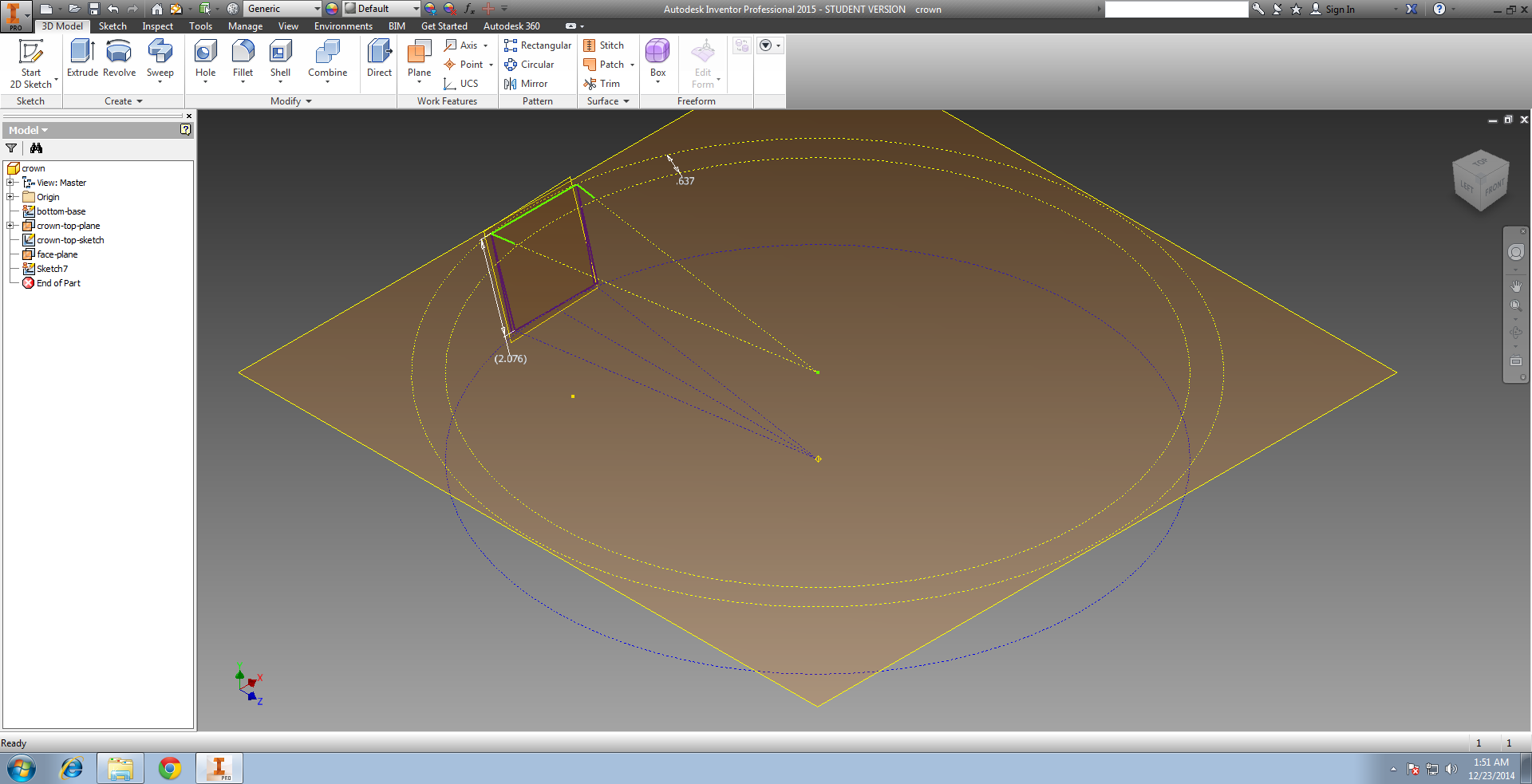
While basically insignificant on it’s own, that gave me the number of panels I’d need to generate, along with the angle that each one would have. I grabbed the face from that, printed it out a couple dozen, and generated the first physical model made of paper and tape.
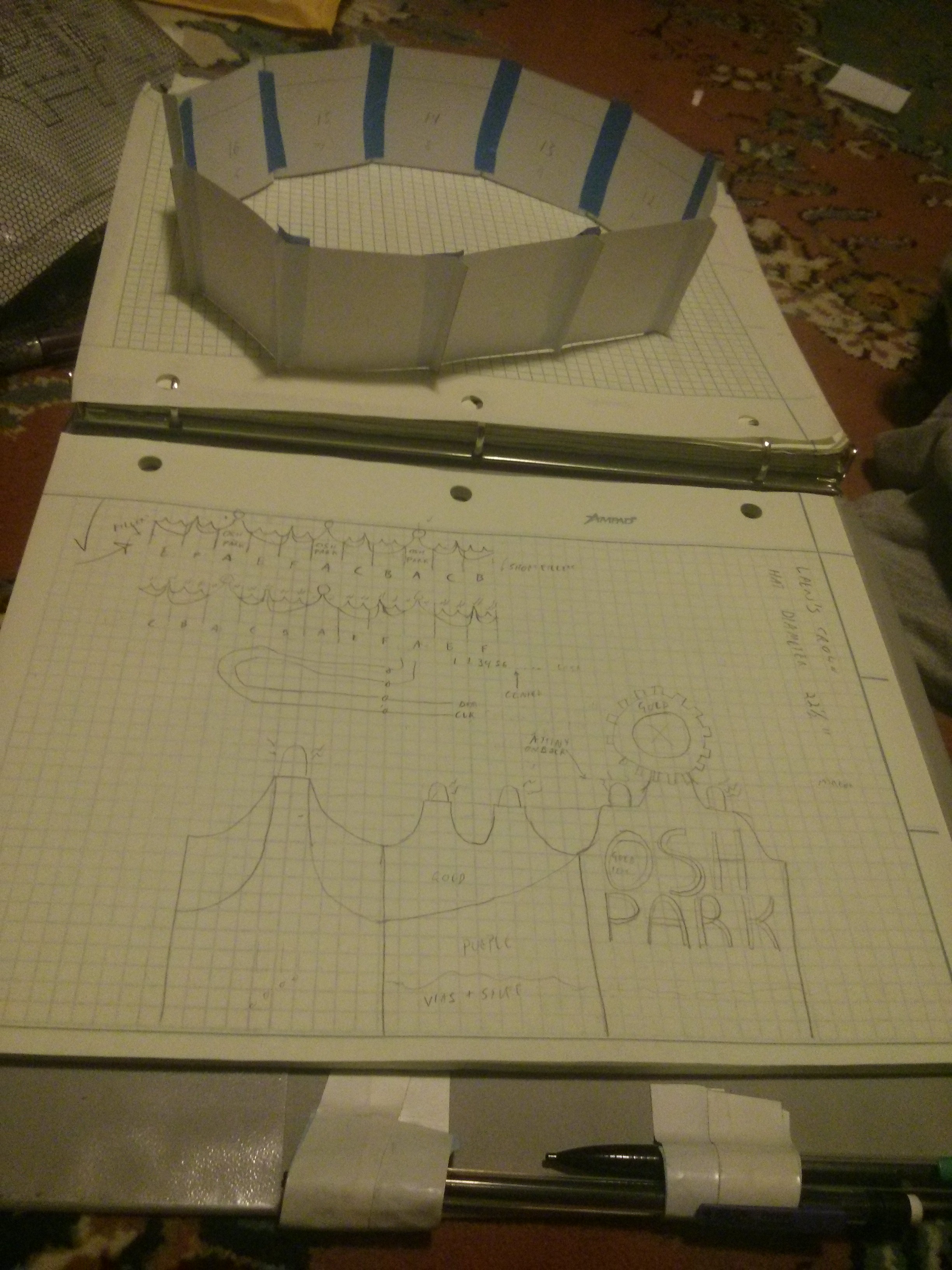 You’ll also see all the drawings I did to get the feel for the crown’s shape. The angle really looks nice on the paper, and keeps it from feeling flat. Since the boards would come out in sets of 3, it was critical that the design be repetitive enough that I could reuse panels, but add enough contours that it didn’t feel repetitive. Since I also wanted to wire up LEDs to the top, I also needed something that could prop up the “gem” LEDS in a consistent fashion. The dual swooping shape seemed to give me the feel I wanted, while maintaining a consistency for the LEDs, and allowing for a larger front face to blast the OSH Park logo.
You’ll likely notice that between this initial design and the final one, I didn’t totally honor my initial drawing, and opted for each panel to have 2 LEDs. After some experimenting, I found that a single one left an inch and a half on each edge, which looked really inconsistent when looking at it from a lighting perspective, even though it looked great on paper (literally).
You’ll also see all the drawings I did to get the feel for the crown’s shape. The angle really looks nice on the paper, and keeps it from feeling flat. Since the boards would come out in sets of 3, it was critical that the design be repetitive enough that I could reuse panels, but add enough contours that it didn’t feel repetitive. Since I also wanted to wire up LEDs to the top, I also needed something that could prop up the “gem” LEDS in a consistent fashion. The dual swooping shape seemed to give me the feel I wanted, while maintaining a consistency for the LEDs, and allowing for a larger front face to blast the OSH Park logo.
You’ll likely notice that between this initial design and the final one, I didn’t totally honor my initial drawing, and opted for each panel to have 2 LEDs. After some experimenting, I found that a single one left an inch and a half on each edge, which looked really inconsistent when looking at it from a lighting perspective, even though it looked great on paper (literally).
Layout
Protip: Don’t do this.
The layout for this was difficult for a couple main reasons:
- The limitations of Eagle Light I use in personal projects
- Arbitrary artistic constraints
- I couldn’t stand all the empty space not being used for something.
- Very short timeline (a bit more than a weekend)
The first limit meant that I couldn’t have more than 1 panel per board file. This greatly confounded my ability to just make all of the panels together, and had to do a lot of shuffling back and forth for testing. I got around this in no small degree by making the primary parts of the panel a part footprint, which was tweaked and modified while laying out the first board. The rest was done by drawing the rough shapes, the swoops, and any artistic bits in advance on a single file. Since the Eagle Light limitations only apply to pads and vias, I was able to draw the everything else on the first panel, and make copies of that file to get everything picture perfect.
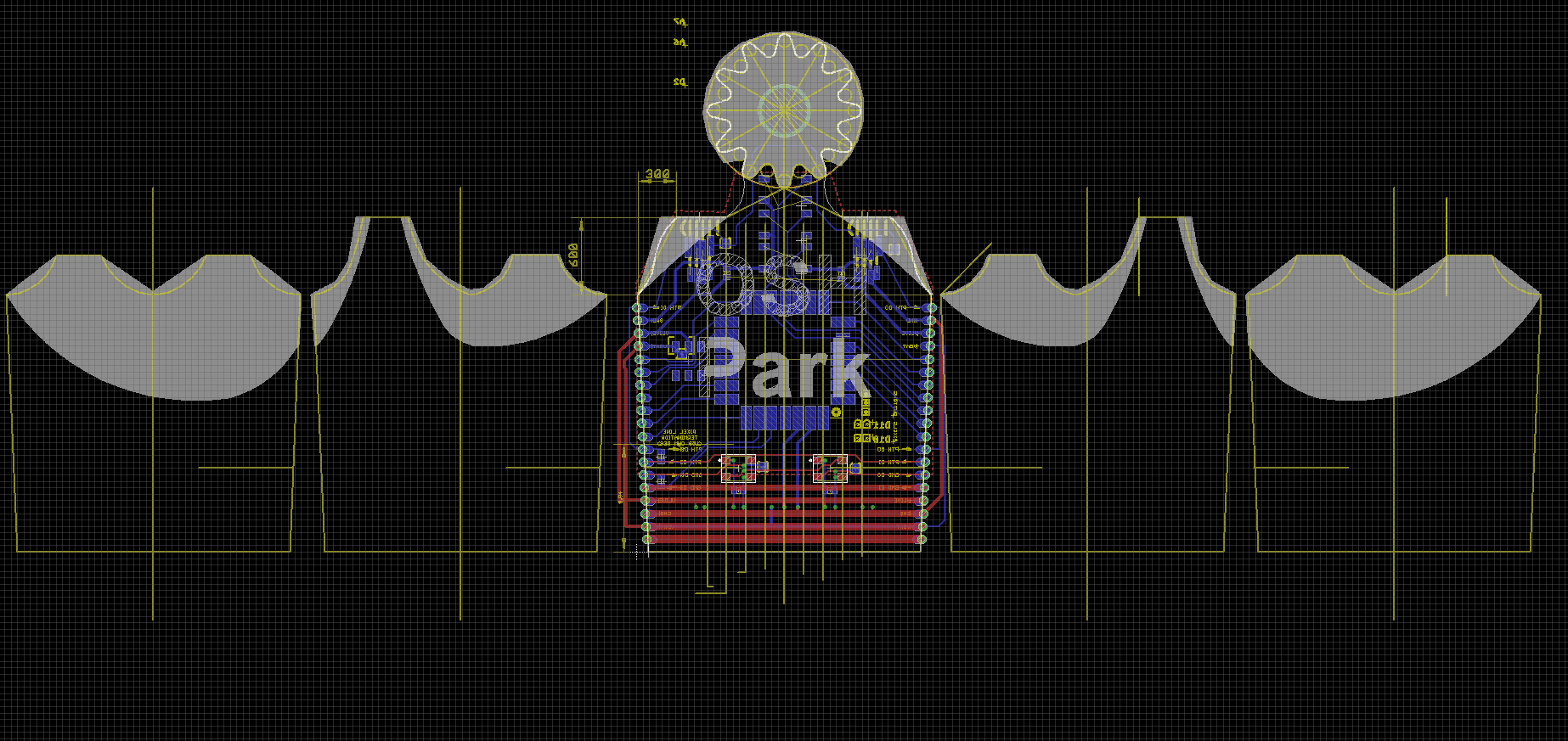
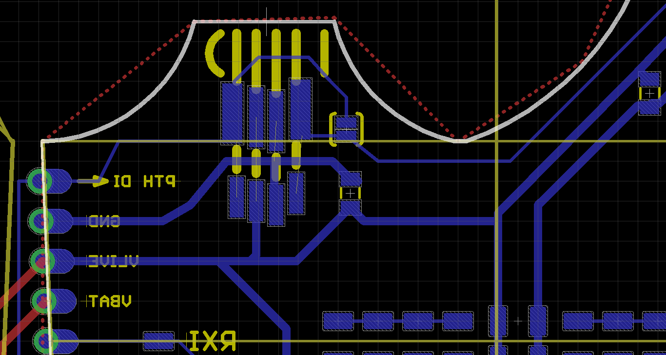
The artistic constraints added some unusual bits. Since I planned for the top of each crown to be gold, that meant I couldn’t solder the LED using vias. That means, the only way to get my 4-wire PTH LED attached, is by faking it as a surface mount component. This seemed like a good idea at the time. In practice… less so. That’s covered in the Lessons Learned, if you want to see how it worked out.
 The artistic constraints also forced me into avoiding vias for most of the rest of the board as well, which made a lot of routing really, really tedious. Aside from this footprint though, most of it wasn’t brain warping, save for the power and ground. Those are kind of important, so I did the only logical thing I could. I cheated by routing off board.
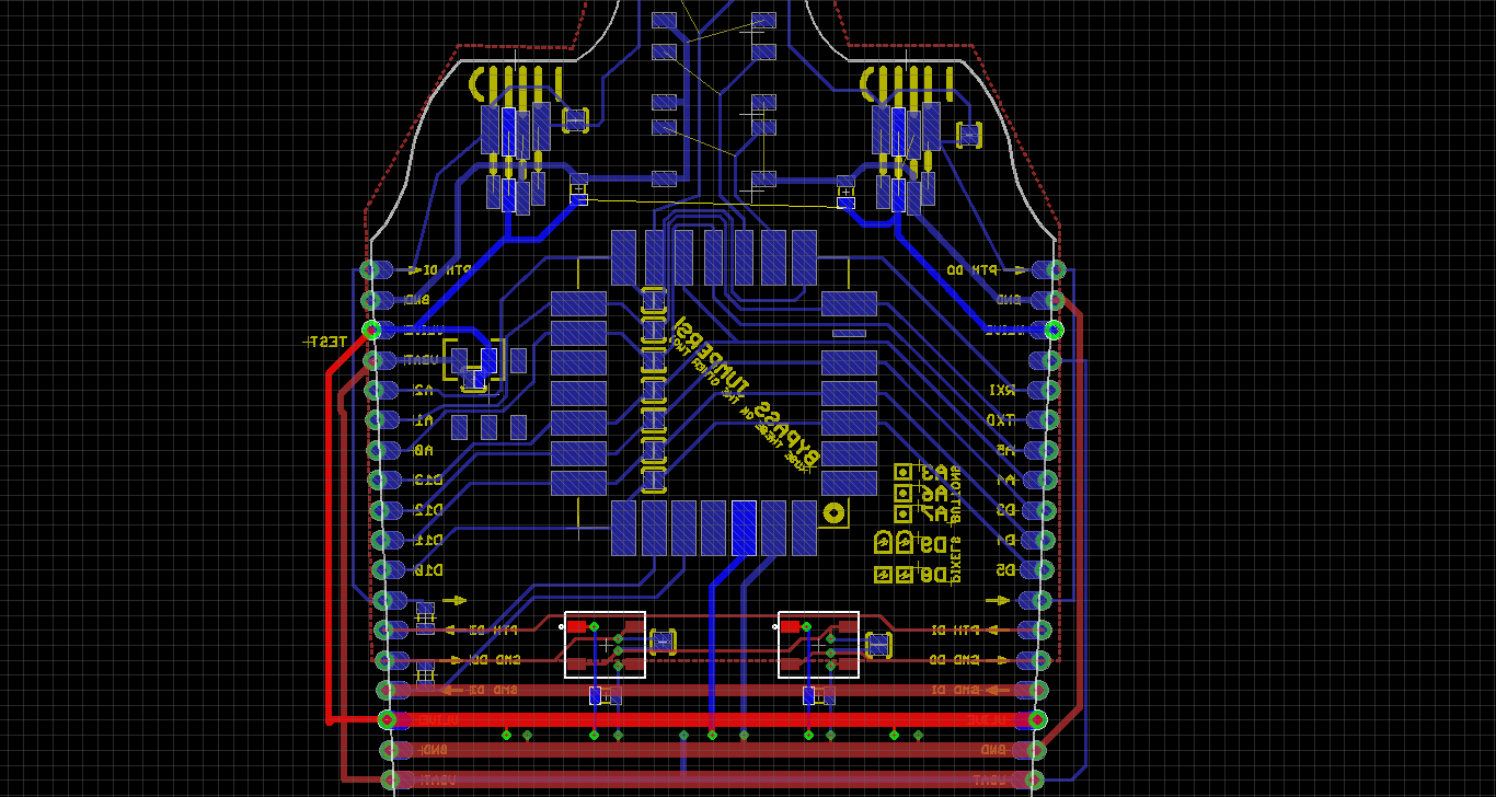 So, the power for half of each top is completed by connecting to the adjacent board. On the face boards you see here, both of the top LEDs are routed off board. This places an extreme dependency on a fully assembled system, but it does save me some vias. Also note that due to the Eagle limitations, this was tested by opening up the adjacent board, and manually cross referencing all the connections.
Speaking of odd constraints. I figured to save coding effort, the first pixel in the chain should be in the back. So, rather than the sane thing of starting where the controller is (which is the very front of the crown), I instead routed the DIN pin on a ring that connects to all the faces. Then, it’s connected to the DIN pin of the particular LED with a 470 ohm resistor, as suggested by the Adafruit Uberguide. Notably, in my routing I left the the DOUT pin on the last pixel, leaving it to feed to the first pixel, which is also being fed by the controller. So, that was a cut trace on the final board.
For the empty space, my initial thought was to add an accelerometer. Since this is a hat after all, you could do some cool things with head movements that way. Since it was also a Maker Faire project, a light sensor would help with lighting changes between indoor and outdoor operation. There wasn’t enough weekend though, so in the end I settled for a psuedo-breadboard for surface mount parts, thinking that maybe it could be added later. At the very least, it’s shiny, and that’s good enough.
I also realized after the whole thing was done that I wasn’t totally satisfied with the gold, since it was very bland. So, I wanted a design to spruce it up. But, it was really late at this point (0430AM, with about 4 hours til the deadline), so I instead opted to use some fancy gerber manipulation instead.
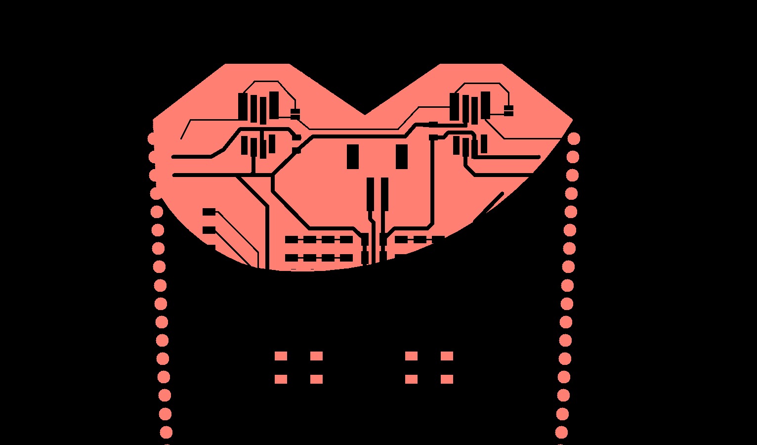 One consistently frustrating thing about design tools is that you can expose a section of the board (usually copper), but you can’t un-expose it. Usually, the in-design-tool way to handle this is draw the whole thing in photoshop, and then import it as a graphic file with the sections you want missing. I won’t have any of that. Instead, I’m taking advantage of the native Gerber commands. Most gerbers (especially Eagle) are written with
 %IPPOS*% meaning that “this is positive, and all these objects are adding to the mask”, which in turn means “expose this part of the board”. However, you can also utilize the %IPNEG*% setting, which means “everything after this is negative and subtracting from what we’ve already drawn”, which is exactly what we want. So, getting really fancy doodles to be drawn in purple is actually pretty simple with that in mind:
- Make the primary layer into a gerber. In this case, the frame for the mask
- Figure out what you want to subtract, and put it in it’s own gerber. In this case, it’s the copper layer from the reverse side of the board.
- Open up the subtracting layer in a text editor, find the
%IPPOS*%, and replace it with%IPNEG*%. Sometimes these are labeled%LPD*%and%LPC*%, which means the same things (short for Layer Polarity Draw and Layer Polarity Clear). - Open the files up in GerbV, and go to File > Export >RS274X Merge, and save it as a new file. It’s helpful to note that at this point, you can’t actually see the subtractive gerber, because there’s nothing to subtract from yet.
- Open the file, and look at your handiwork! Or, look at the same initial imagee. One of the two It’s also very helpful to note that the merge is order-dependent. The layer on the top should be the primary, and the bottom one the secondary (or, vice-versa, it’s been a while). If it didn’t subtract, flip the order in the Layer pane and try again.
And, you’re done! You can also stack the Clear and Draw layers, and continue to merge things for more elaborate designs. It’s not advised to get too crazy though. I’ve heard some tools start getting angry when you have more than a few polarity stacks.
Secrecy
This was actually one of the more tricky parts. Since this was a surprise, we really wanted to not let Laen know in advance. However, laen’s personal commitment to quality makes this tricky. Partly because he looks over the panels for any oddities, and also because this says OSH PARK in huge letters on one board. Submitting the board was easy enough: Hope he doesn’t look at the stop mask layers (which never have problems anyway), and by ordering really early in the morning on a Monday, so he’ll be incredibly busy and hopefully not perusing for interesting designs. Fortunately, by themselves, most of these are actually really uninteresting, and the mildly interesting one is pretty bizarre and hard to extrapolate a purpose.
The second, harder part: Getting it off the panel. Fortunately, Cat and Kelly helped out on this one. We kept in contact on when the board would arrive, and Cat distracted him with questions while Kelly ripped the panel apart and snagged all the boards before he looked it over. Good work team!
Assembly
This is the storytelling portion. For instructions, go to the Assembly page. And good luck, you’ll need it.
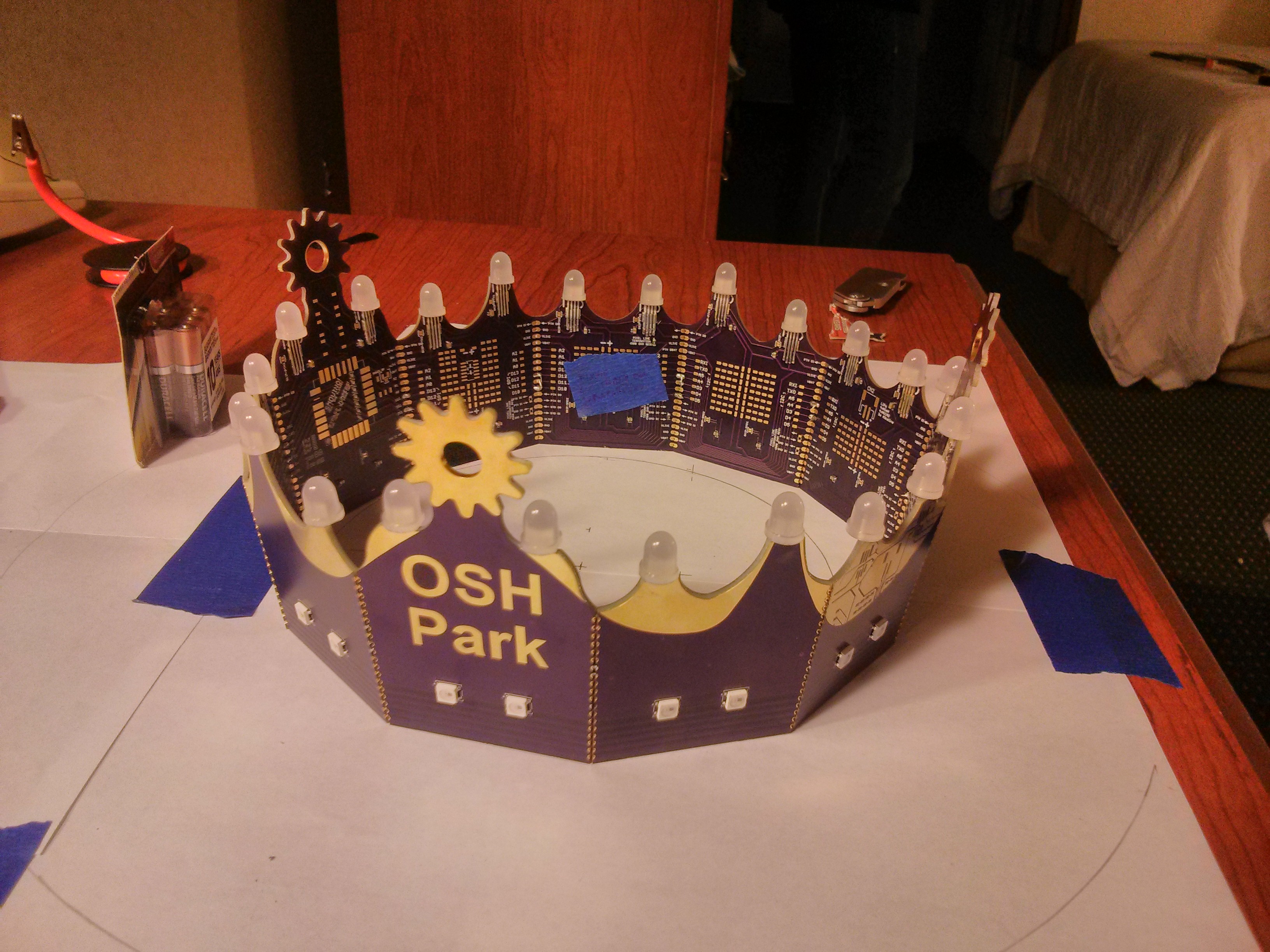
First thing I did when the boards got back was lay them out, and see what it was going to look like.
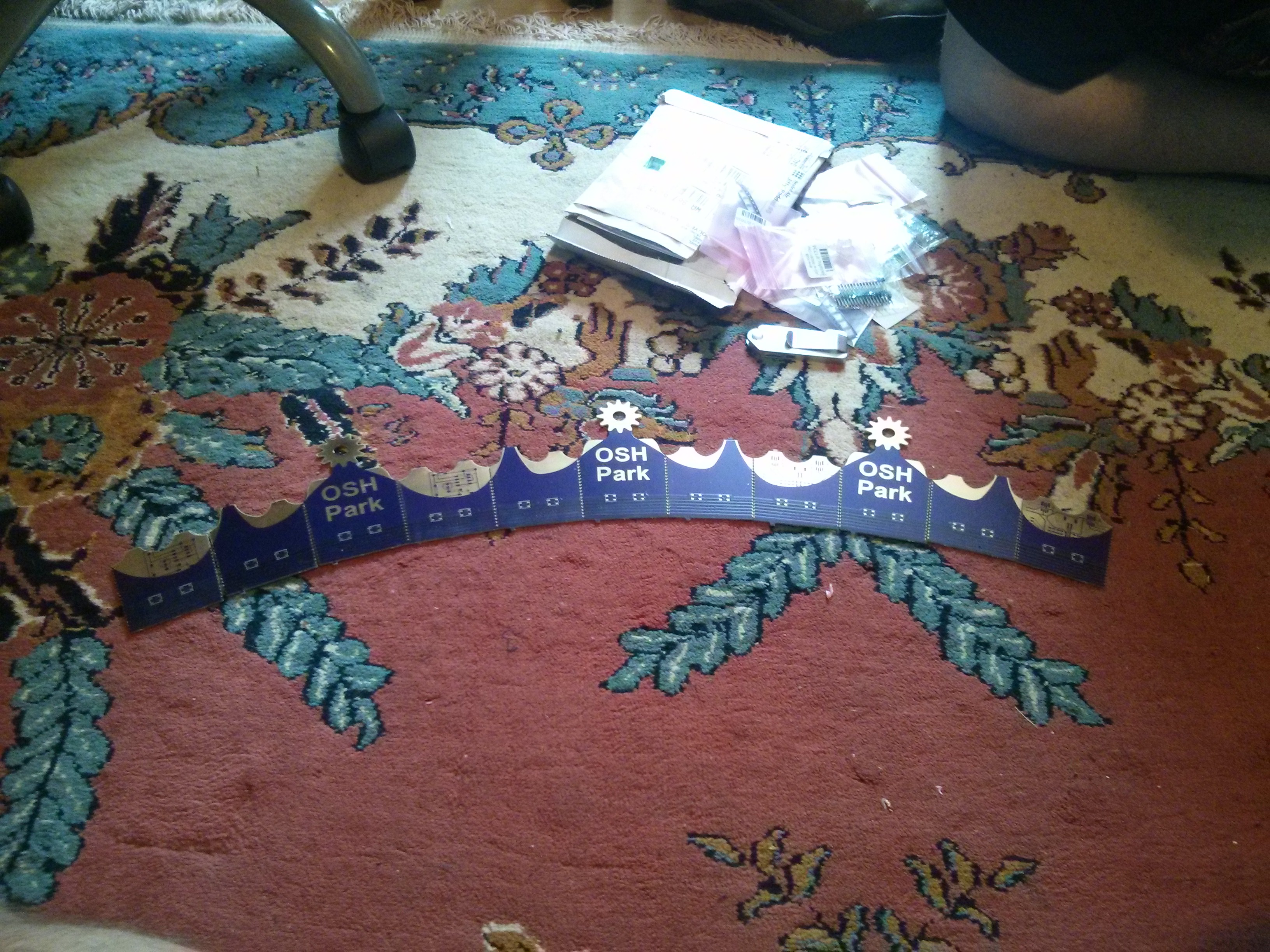 So far so good! Next step was cleaning up the edges. Castellated edges aren’t really pretty coming straight from a fab. The router basically mashes the via plating (which is thin and flexible) into the cavity or into the next connection. There’s a total of 570 such connectors on this project, so ensuring that they were fit for building took a couple hours.
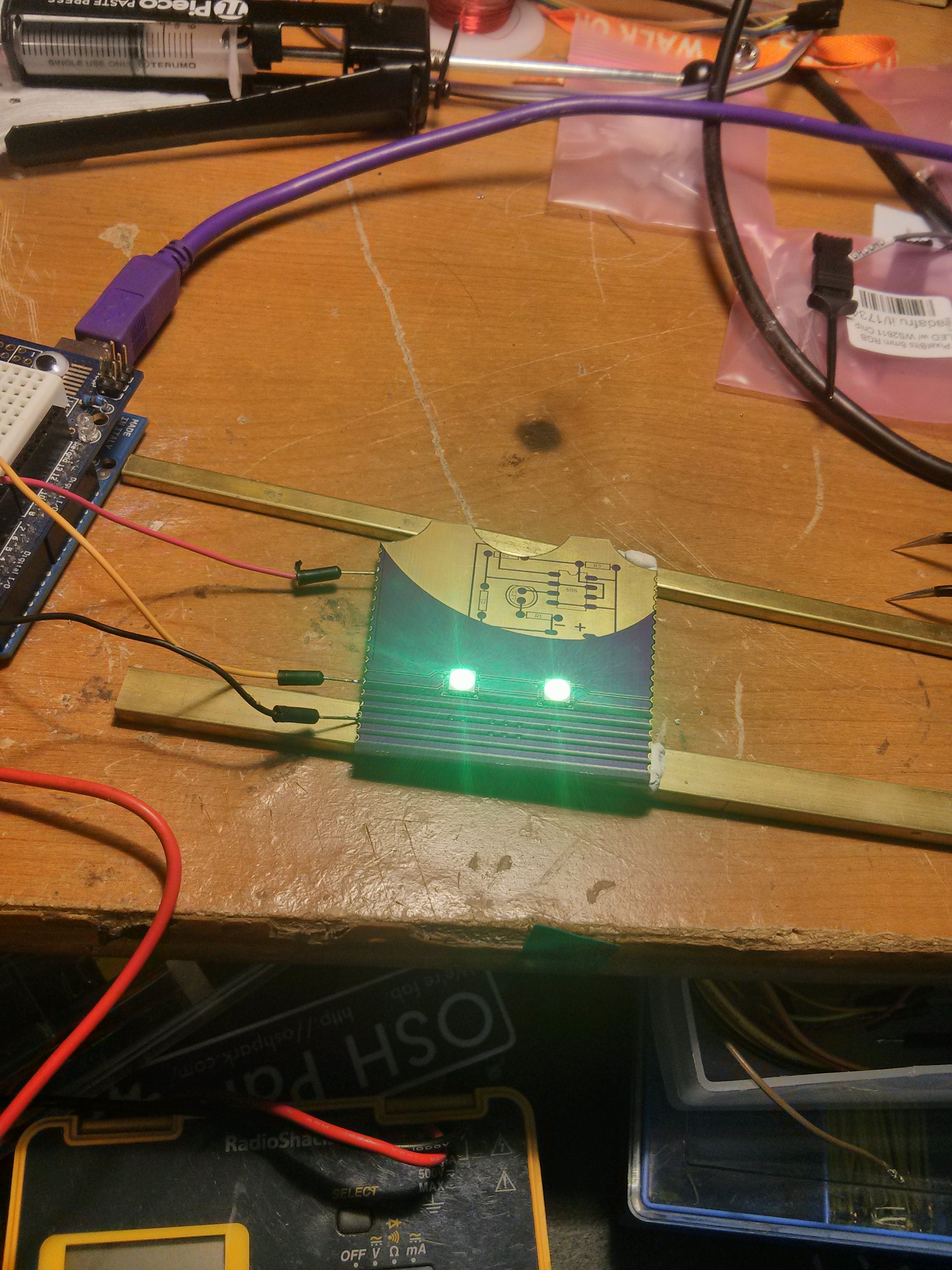
Eventually though, everything got cleaned, and I assembled the first board to see if there’s any hope of it actually working. Fire it up, and NOPE. Turns out, the LED footprint that I had gotten from Adafruit had the dot in a weird location, so I assembled it backwards. Reversed the LEDs, and fortunately it resulted in this:
 This was then repeated 13 times (I needed 11 panels, but built some spares just in case) and the SMD part was completed.
The tricky bit of assembly was attaching the the surface mount ones. During this process I discovered an amazing partner in pcb assembly: Poster tack. Forget all the talk about panavises, actual vices, and assembly jigs. Put a blob of poster tack on your table, and you’re golden. I found this out when trying to assemble the blasted through-hole LEDs as surface mount parts. I wound up making a small cradle for the LED, and then squishing it flush to the board for my first pin. After that, I could manipulate it a bit easier, and have some level of success tacking them down. It’s incredibly safe to say that this project would have not been completed without poster tack.
At this point, I just did part-by-part testing. One critical note on this project is that we were giving it to Laen to wear around Maker Faire. As a result, it would be traveling to California via airplane. So, assembling the full kit in advance poses not only a lot of danger to it with the baggage handlers, but also takes up a lot of precious space in luggage. So, it was determined that we could assemble it in the hotel room.
Assembly, Part 2: Hotel, California
Upon arrival in Cali, Kelly, Cat, and myself started planning for the assembly process. I had brought the tools, and Cat brought some bits to make the product more comfortable when assembled. I did make one critical mistake, which was that rather than risk my good Hakko iron in an airplane, I grabbed my roommate’s cheap fire-starter iron. One thing I really didn’t take into account was that it said “Hobby Iron” on it. Not “Soldering Iron”. So, I learned, in this process, that flux and unleaded solder will dissolve brass. So, while we were going through the already complex assembly process, the tip was literally vanishing into the crown.
Anyway, the process was mostly simple. We drew a large circle on paper, and tried as best as possible to line the parts up tangent to it. Kelly has really steady hands from depanelling boatloads of circuit boards every day, so she held the parts together while I tried to tack them together with little bits of solder. For the first 3 or 4 panels, we were simply trying to get the thing to support itself, to various degrees of failure. Eventually we grabbed a battery pack from my briefcase, and used that to help sturdy one side (I forgot poster tack, which would have been useful), and were able to get it half-assembled pretty quickly.
The other half proved very difficult, and required a lot of minor rework to make the whole thing actually circular. We wound up going through most of the connections 3-10 times to get the last couple connections hooked up, and in the end ripped off a few pads. For one board we simply replaced it, but one pad was on the tall OSH Park panels, which had no spares. We had to bypass the bad pad bypass that with a jumper wire for that one. (Yes, it was a purple wire. We’re not savages.)
Once we got to this point, it was a bit simpler. Just solder it together, with Kelly helping support the very fragile connections. The only major issue at this stage was when we noticed the solder tip have entirely vanished. At this point, we had to wait for the iron to cool in order to use a new tip. All in all, we lost 2 brass hobby tips to the connections on this.
So, the assembly was completed at Sunday evening of the Maker Faire weekend. Or, if you do the math, immediately after Maker Faire. So, our initial hope of Laen wearing it was dashed. However, the incredible fragility made that pretty obviously not reasonable anyway. However, we did have the Bring-A-Hack dinner! Which is a nice, sit down place anyway. With a bit of rushing, we actually completed this 10 minutes after the start of the Bring a hack, walked there, and were fashionably late, with a gloriously blinking box to Laen’s utter surprise and joy. The two best parts about the delivery:
- After Laen’s shock at the crown, someone asked “Is it supposed to be smoking?” which definitely highlighted that this was the right place to unveil the project.
- After the crown was gently doffed and confirmed to not be on fire, Laen declared “Man, I was so excited about my box, and then you guys do this…” and holds up a small cube made of solder-together boards.
To be fair, his box is far more durable than the crown, although it does lack blinky lights.