PCB Crown::Lessons Learned
As my first run at 3D circuits, there was a great number of assumptions that I was totally wrong about, and a few things that I had never even considered. But, the math did work out, so at least there’s that.
Avoid having structural components carry signals
This is one of those lessons that’s 100% obvious in hindsight. My initial assumption was that if it holds well enough to provide structural integrity, it’ll hold well enough to provide current. That’s true, but what I hadn’t considered was that good signal lines need to be connected to things, and relatively small. However, structural components can be big nasty blobs, and that can help them do their job.
If I were to do this again, one of the things I would do is put really large pads on the side, to really get a good solder blob on there. And then, just not connect it to anything. That would have made assembly a great deal easier.
The other reason for this is simple: The first few joints in a 3D model may need to be tweaked and reheated several times, which is not good for your connections. Having dedicated structural stuff means you don’t have to worry about potentially over-stressing a trace.
Castellations work, but mind the placement.
The castellation method of connecting the joints together did work great to an extent. One of the most significant failings was simply that stressing the joints ran the risk of ripping the via plating off of the substrate. The issue is that unlike the top and bottom copper layers which are literally glued down, the via plating is held on only by a weak bond from the plating process. That’s it. So, they turn out to be less durable than one would hope for. To compensate for this, there’s a couple tricks we can do.
The first one is to make sure that any support structures include a lot of top/bottom copper in addition to the via. This gives you a good solid place to connect. However, this provides only marginal benefit over using the copper layers, and excluding the via entirely.
The second option is to castellate the via, but only slightly. This picture should help clarify:
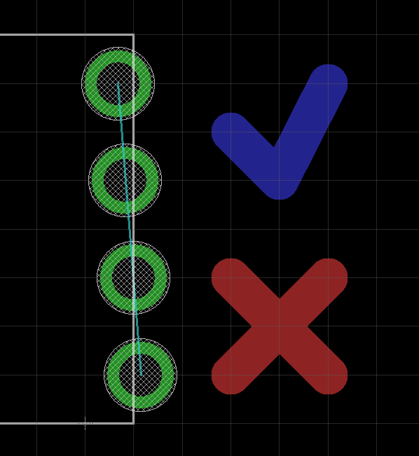 The reason for this is simple: The plug formed by the solder is now thicker than the edge of the board. So, now instead of being held by magic, there’s a real physical barrier in the form of the substrate. This makes the weak via plating much less significant. But, what about just not castellating it at all? What about just moving the whole via in a bit, and not cutting it off? That’ll probably work great too. For 90 degree corners, this will probably work great. For obtuse angles like this though, placing the vias that far inward might start moving the via into a less structural placement, and force the top pads and backing adhesive to do the heavy lifting, instead of the solder itself.
If at all possible, make each component easily testable and self contained
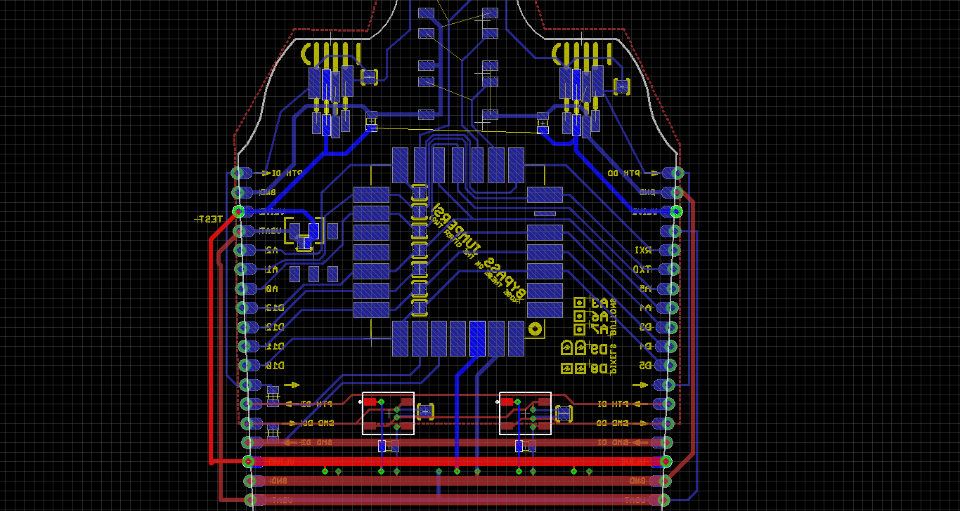
This was something I was totally unable to do due to artistic concerns, and it caused a bit of anxiety during assembly. See, because each piece relied on the whole system, it was really hard to tell what went wrong. Any time something started going haywire, I had a multitude of connections to verify. Here’s an example of it:
 Why didn’t I just connected it to the ground plane on the other side? In this case, because the top side
Likewise, because this had a neopixel strip designed in, data was actually sent serially around the crown. Once the connections started giving out, you wouldn’t believe the data corruption that started happening as each connection got mangled resulting in all sorts of absurd color patterns. A lot of the time though, it just froze. this was
Don’t try to dual-purpose a component lead as a signal wire.
This was one of those things I had originally intended to do, realized it was a terrible idea, and fortunately was able to work around in most scenarios. However, there’s still a few places where things work better if I have a mysterious jumper-lead. One of them is shown in the picture above: There’s some buttons on the top that connect the ground lines from the two sides, and also shorts out a signal line if you press the button. There is a ground plane on the reverse side to eleminate this, but trying to test this module without the button was a headache.
Watch your line termination
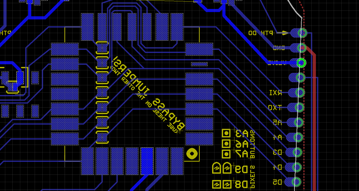
This is something I vaguely anticipated, then promptly thought I had fixed when I hadn’t. The front side of the board has several lines that form a large ring around the entire crown. My idea for the design was to use the 50 ohm resistor suggested by the Neopixel Guide as a jumper, which brought the pixel data line from the Atmega chip to the first Data In pin on LED0. However, what I hadn’t really fully thought out is that this did terminate the data-in line properly, but the data-out line still bypassed it, and fed the next chip. Dangig! So, on the back of the crown, I had to carve out a trace very carefully to correct this.
If I were to do another design like this, I would include a special plate for the back that handles all the line termination, and jumpers everything together. Attempting to design in a “bypass” mode in my case caused erratic behaviour due to the one forgotten line.
Put all connected parts on the same design
Since I use Eagle Light for design, this limitation made the design much harder to sort out. If at all possible, make sure your design tool will permit you to work with the full size of your project. This might, in fact, be a good time to switch to KiCAD.
Hobby Iron vs Soldering Iron: Not the same.
Since the plan was to assemble this in a hotel room, and I didn’t want to risk my good soldering iron going through a flight, I borrowed my roommate’s that he had lying around. I figured a firestarter would do the trick right? Nope. This was an actual woodburner, complete with actual brass tips. Turns out, those will happily dissolve into solder when assembling circuit boards. This particular project had enough solder joints that it converted 2 pointed tips into tiny nubs before we got everything attached.
Make a jig, or at least a good assembly guide.
This one totally caught me off guard when we assembled this. I was having one heck of a time holding the parts together, and had absolutely no angular references to speak of. Worse, since this particular project also tilts outward, it had a very real inclination to fall over at the slightest provocation. In the end, with the secret underground project cabal (eg, my wonderful coworkers), we got a system to get it going. Kelly held the boards together, I tapped the solder joints in, and Cat provided the odds and ends like helping with solder, helping hold heatsinks to the boards, and providing the 5th and final hand needed.
Not all lessons were failures
There were, fortunately, a few things I did actually get right.
Plan for failures
Next to every LED, I added in a small bypass jumper. The idea was that Laen would be wearing this all day at a convention, and one of the lights might give out, and we could do a quick fix by shorting the data-in to the data-out. Well, that did happen. The PTH LEDs that I held down with a SMT footprint had some solder attachment issues. A few of the LEDs required the “top” pad to be fully connected, and due to the weird placement, it was hard to get without causing shorts on the adjacent pins. More often though, the issue was simply that the connection between two LEDs was broken. Soldering the jumper ruled out the possibility of the LED being at fault, and often made connections simpler to troubleshoot.
Make a project specific library
Rather than clutter up my library with weird, random parts, or accidentally modify a known good footprint, just tweaking them helps a lot.
Poster tack
A surprise discovery is that poster tack is an invaluable tool when assembly circuit boards. It works amazingly. It holds the board at the table level. You can use a blob to prop it up to help with lighting. You can take a blob and jam it on a part to hold it still while you solder. You can also, if need be, make a small jig with it and cradle large parts. And, critically for art boards: It not only leaves no mark, and actually removes finger smudges. Shockingly, it also holds up pretty well to a heat gun, and will last for quite a few boards when doing SMD rework when heated to rework temperatures.